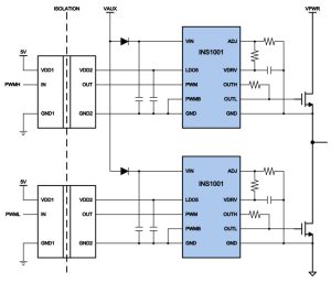
The single-channel INS1001DE is intended to supply fast powerful voltage-regulated waveforms to the gates, which are extremely sensitive to over-voltage stress.
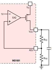
Its output pulse amplitude is set by a low-drop-out regulator using two resistors, to, for example 6V which is commonly specified for enhancement-mode GaN hemts (diagram below right).
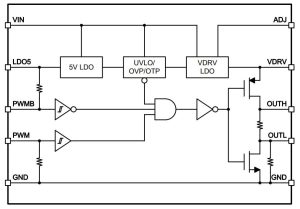
A separate internal LDO provides 5V for the internal logic, from an external supply of 6 to 20V.
No isolation is included, but 5V is provided out of the IC to supply an external front-end digital isolator.
The output stage has a 1.3Ω pull-up and 500mΩ pull-down, with separate pads to allow separate pull-ip and pull-down resistors to set turn on turn-off times.
Into a 1nF gate, typical rise-time down to 10ns are available, and fall-times down to 3ns. Propagation delay through the device is 35ns (50ns max).
 Regardless of supply voltage, the two logic inputs have the upper and the lower thresholds of 2.8V and 1.2V to make them compatible with 5V and 3.3V logic. One input is inverted to allow PWM or /PWM signals to be handled, and a de-glitcher at the chip’s inputs will not allow pulses less than 15ns wide to affect its operation.
Packaging is a 3 x 3mm DFN3x3-10L with thermal pad.
“The INS1001DE is perfectly matched to optimize the performance of e-mode GaN HEMTs, and particularly innoscience’s e-mode InnoGaN,” said the company’s v-p of IC design Min Chen.
 Electronics Weekly Electronics Design & Components Tech News
