9th May 2023
Automotive Electronics, Career Advice, Device R&D, Internet of Things, Materials R&D, Medical Electronics, News, Sensors, University Electronics
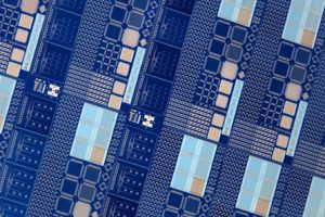
Melexis is encouraging innovation and drawing on the rich pool of local technology graduates at its newly-opened Innovation Lab. Positioned in the Swiss canton of Neuchâtel, the Melexis Innovation Lab is the latest addition to the Belgian company’s site in Bevaix, near Geneva. The lab was opened in December 2022 and is a centre for pre-development of sensor technology products ...
18th November 2020
Automotive Electronics, Business, Design, Device R&D, Embedded Systems, Industrial Electronics, Internet of Things, Markets, Military/Aerospace Electronics, News, Process R&D, Research
EDA company, Mentor, has joined Nano 2022, the latest project to promote the French electronics manufacturing industry. It covers components, connectors and PCBs, to design and assembly, distribution, embedded software and software tools. The project is part of the European Commission’s Important Project of Common European Interest (IPCEI) to promote research and innovation in power ICs, sensors, optical equipment and ...
27th November 2018
Device R&D, Medical Electronics, News
Photonics has been called one of the fastest developing areas in healthcare.
4th May 2018
Device R&D, News, University Electronics
Three UK universities are to take part in a £11m programme for the development of nanotechnology for electronics. Imperial College London and the Universities of Southampton and Manchester, will work with industrial partners on the project to replace traditional transistors with memristors as the basis of electronic circuits. Today all ICs are built from vast numbers of transistors (electronic switches). ...
24th April 2018
Device R&D, News, Research
A professor at the University of Sussex has been given the job of making the UK a world-leader in sound shaping technology. Professor Sriram Subramanian has been named a Royal Academy of Engineering (RAEng) chair for the development of novel acoustic interfaces. This is one of a ten areas of development emerging technology being created by the RAEng, which is ...
7th March 2018
Device R&D, News
CST Global, the Glasgow semiconductor laser manufacturer, says it is sampling its 1270nm, 2.5Gbit/s asymmetric and 10Gbit/s symmetric, DFB lasers for 10G PON (passive optical network) applications. The firm is currently beta sampling its asymmetric 2.5Gbit/s lasers and alpha sampling its symmetric, 10Gbit/s lasers. The asymmetric beta samples, which are undergoing ITU-GR468 reliability testing, are available for customer trials in ...
19th January 2018
Device R&D, News
Next week at SPIE Photonics West in San Francisco, French research centre Leti will demonstrate a new curving technology for optical components that widens field of view and compensates for optical aberrations. Called Pixcurve, it is a proof of concept for optical components such as microdisplays, visible imagers and cooled infrared sensors used in mobile phones, telescopes, medical-imaging tools, IR ...
18th October 2017
Device R&D, News
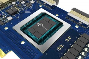
Intel says it will ship its first silicon for neural network processing before the end of this year.
6th October 2017
Device R&D, News, University Electronics
Scottish scientists believe they have made an important discovery in the practical application of high-speed photonic circuits.
21st September 2017
Device R&D, News
A government-funded research project to develop semiconductor lasers for the design of miniature atomic clocks (MacV) receives new funding.