It would “enable chip designers to produce ICs in older 180nm, and even one micron, geometry fabs with the equivalent performance of CMOS devices made in state-of-the-art plants”, according to the company. “For example, a fab equipped with 180nm photolithographic steppers could now produce devices with the size, speed and performance of 35nm CMOS.”
Behind its claims are the company’s novel tunnelling transistors (now branded Zpolar), a manufacturing process (dubbed Bizen) which makes the transistors on old CMOS fabs, and a few-transistor low-data-voltage non-complementary logic system using the transistors (branded ZTL).
Area gains over CMOS, according to the company, are due high transistor conductivity leading to small transistors, and fewer transistors – most ZTL logic gates have only one – which reduces the need for space-consuming conductors within a logic cell. Read further down for more technical detail.
Characterisation has allowed SFN to announce four IC design packages, branded ITMs. The company describes them like this:
- ITM180, which can deliver chips with the performance of 180nm CMOS using one micron equipment
- ITM35, which enables 35nm CMOS-equivalent ICs to be made in 180nm process node fabs
- ITM5 which enables 5nm CMOS performance from 28nm steppers
- ITMSubnm which means that current state-of-the-art 3nm fabs will be able to deliver sub-nm, Angstrom-level capabilities
“VHDL is taken into the selected ITM – dependant on performance requirements – from chip designers,” it said. “The ITM, which contains the fully-characterised LIB [device libraries] and PDK [process development kit], supplies both the POR [process of reference] and GDSii information to the foundries to make the ZTL chip.”
Can we have a practical example?
SFN has produced a theoretical comparison using a 0.35μm CMOS Pentium 2, and an equivalent ZTL device optimised in three different ways:
| CMOS 0.35μm Pentium 2 (Klamath) | CMOS Pentium 2 Scaled to 1μm | 1μm ZTL speed matched |
1μm ZTL power matched |
1μm ZTL linear speed/power |
|
| Average transistors per logic gate | 7.5 | 7.5 | 1 | 1 | 1 |
| Transistor count | 7.5m | 7.5m | 1m | 1m | 1m |
| Supply | 2.8V | 5V | 2.7V | 4V | 4.2V |
| Vhi-Vlo at capacitive load. | 2.8V | 5V | 260mV | 210mV | 180mV |
| Max clock | 300MHz | 38MHz (8x drop through capacitance) |
38MHz | 380MHz | 1GHz – 3GHz |
| Rise | 310ps (est) | 2ns (est) | 1.82ns | 278ps | 45ps |
| Fall | 310ps (est) | 2ns (est) | 2.24ns | 242ps | 47ps |
| Propagation | 0.95ns (est) | 7.5ns (est) | 574ps | 76.4ps | 12.5ps |
| Active power per transistor | 5.73μW | 5.73μW | TBC | TBC | TBC |
| Total static power | 0.1W | 0.1W | <0.1W * | ||
| Total active power | 43W | 43W | 3.1W | 42W | 510W |
| Average gate area | Approx 8:1 | 1 | Approx 20:1 | Approx 20:1 | Approx 2:1 |
| Die area | 1/8 | 1 | 1/20 | 1/20 | 1/2 |
| Layers/risk | 24 (est) | 24 (est) | 8 | 8 | 8 |
| Theoretical fab lead time | 39 days (est) | 39 days (est) | 7.5 days | 7.5 days | 7.5 days |
| Actual/ manufactured fab mode |
0.35μm | 1μm | 1μm | 1μm | 1μm |
| Equivalent fab node area saving /infrastructure time shift |
0.35μm +5 years |
1μm 0 years |
0.18μm +10 years including interconnect saving |
0.18μm +10 years including interconnect saving |
0.18μm +10 years including interconnect saving |
| Die area cost | 1/8 | 1 | 1/30 | 1/30 | 1/3 |
| Fab time cost | 1 | 1 | 1/5 | 1/5 | 1/5 |
| Fab geometry cost | 8 | 1 | 1 | 1 | 1 |
| Total cost | 1 | 1 | 1/150 | 1/150 | 1/15 |
* If 2.5% of the logic was left powered with a 15 fold reduction in power consumption, static power would drop from 43W to 72mW.
(Editor’s note: if this table it too wide for your browser, copy it and past it into a document)
Cost figures in the table are based on SFN’s Bizen simplified in-fab wafer processing, which can run on standard silicon process technologies using standard CMOS processing equipment.
“A 180nm fab using ITM35 delivering ZTL chips with the equivalent performance of 35nm CMOS will have ten times fewer process steps than an actual 35nm CMOS process, resulting in a 10 fold reduction in production time,” said Summerland. “This translates into a 40-50 fold increase in net profit for the Bizen-converted fab.”
On request, he put numbers to this step reduction: 500 for 28nm CMOS and 50-80 steps for Bizen.
And how long Bitzen take?
“The fab infrastructure installation of the ITM is typically six months,” Summerland told Electronics Weekly. “At the point the foundries have finished their conversion, they would have the ability to provide the abstract cell based tools necessary to turn existing design files – Verilog, for example – into ZTL designs.”
What is this logic?
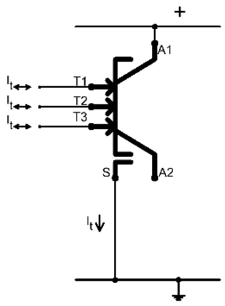
Up-to-date diagrams of SFN transistors and logic have yet to be revealed, but SFN did release a symbol for a three input NOR gate in 2019 (left).
“It’s not exactly correct, as ac tunnel currents are involved and different switching characteristics of the Zpolar transistor,” explained Summerland (see figure below right).
 Transfer characteristic:
Input (blue) moves from logic 1 (325mV) to logic 0 (375mV), causing the output to swing from 0 to 1. The next inverter output (red) shows the high transconductance
“To help explain, the Zpolar transistor has transconductance which neither a bipolar PNP BJT or unipolar MOS can get close to. The ZTL gate’s output is loaded in part by the tunnelling current but mostly by an ac tunnelling component. The transconductance and ac-dc tunnelling allow a single transistor logic to act as a balanced drive, and there is no shoot-through current.” see current and voltage graphs below.
 “ZTL switching currents shown are not like PMOS or RTL, they are like CMOS” – Summerland.
The logic gates are formed by a single transistor that has inherent tunnelling within its structure. Both a NAND and NOR gate are formed from a single transistor, with different tunnelling configurations, Summerland told Electronics Weekly.
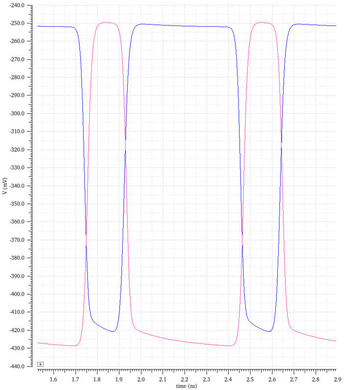 ZTL voltage waveform – with asymetric PWM input
He went on to explain: “ZTL has a high impedance input with a hair trigger, paired with a low impedance output [see transfer function above]. The input-output voltage range is centred around the hair trigger which produces a snap output, which grants good noise immunity [see voltage waveform right].”
“The speed enhancement is due to the phenomenal transconductance of the Zpolar transistor,” explained company CEO David Summerland. “When combined with tunnel mechanics, which applies constant current to transconductance, this gives you huge voltage gains – up to 1000.”
Where has this come from?
“Bizen has been in development at a UK fab for four years, and SFN has produced ‘gold standard’ test wafers, which have been charactericed,” said SFN. “The extracted characterisation data has been put into a JMP data book and used to produce SPICE models which run in the Cadence design environment, and matches the results from the Synopsis wafer process flow.”
The company has also described high-voltage Bizen-based devices
SFN was founded by David Summerland (CEO) and Sam Lodh (COO) in 2016, and is based at The University of Nottingham Innovation Park. It holds 34 patents and currently has ~50 private investors – investors “have already been able to trade their shares off-market at $100m current valuation”, it claims.
SFN’s website is operated by its trading arm Wafertrain
Dear reader: This technology has prompted much head-scratching at Electronics Weekly Towers.
Edifying comments (below) would be especially welcome.
Electronics Weekly Towers: maybe use Head & Shoulders shampoo? 🙂
Morning Bill Martin
You have confused me with that comment
(UPDATE – it took a colleague to point out that you meant the need scratching 🙂 – no one ever accused me of having a sense of humour…. )
FYI, this patent may or may not be the technology involved – we cannot tell for sure
https://patents.google.com/patent/WO2022123261A1/en
(download the pdf version for diagrams)
it seems to fit the presented information
Anyone for a turbo encabulator https://www.youtube.com/watch?v=MXW0bx_Ooq4
🙂
Let’s hope not