
Figure 1: Scanning electron microscopy image of a gate failure. (Dielectric breakdown is observed between the gate metal and the field plate metal)
Gate overvoltage spikes during device turn-on transients are commonly observed in GaN HEMTs (high electron mobility transistors) under high frequency, fast-switching conversion applications. The magnitude of the gate overvoltage transients is primarily governed by the gate loop inductance and the slew rate. Due to the small margin between the nominal gate bus voltage (~5V) and the datasheet maximum specification (VGS, Max=6V), it is useful to understand the gate overvoltage capability of GaN HEMTs and the associated lifetimes.
In this project a comprehensive lifetime equation was developed to account for various gate voltages with their respective duty cycles. Testing-to-fail investigated the underlying wear-out mechanism responsible for the gate failures under overvoltage stress conditions. By understanding the wear-out mechanism, a physics-based model was developed to project the lifetimes under all gate biases and temperatures. Lifetimes including overvoltage spikes and nominal bus voltages are estimated by following common gate mission profiles in real-world applications.
Lifetime equation derivation
The semiconductor industry frequently uses failure-in-time (FIT) as an important reliability robustness indicator. FIT represents the total number of failures per 109 (one billion) device hours. Therefore, the FIT can be generalised by Equation 1:
![]()
where FR is the failure rate (number of failures/time) and t_total is the total time of operation (in billions of device hours).
In real-world applications the devices are likely to experience different stress conditions periodically over the course of the lifespan. Different stress conditions are likely to have different acceleration factors and thus lead to different FITs, as expressed by Equation 2:
![]()
where FITa, FITb, …, FITi are the number of failures from different stress conditions, which can be further expanded by Equation 3:
![]()
where FRi and t_i are the failure rate and the total time of operation under individual stress condition.
By plugging Equation 1 and 3 to Equation 2, it yielded:
![]()
After dividing ttotal to both sides of the equation, it yielded Equation 5:
![]()
The ratio between the duration of each stress condition and the total time of operation is defined as duty cycle, specified by Equation 6:
![]()
The sum of the duty cycles is 100% as shown in:
![]()
By combining Equation 5 and 6, it yielded:
![]()
FR is inversely proportional to lifetime, denoted as LT, leading to Equation 9:
![]()
where LT_Total is the total lifetime, (LT_i) corresponds to the individual lifetime under each stress condition.
The harshest stress condition typically leads to the shortest lifetime. The lifetime term (LTi) is in the denominators in Equation 9. Further, the duty cycle of different stress conditions is included in the numerator.
The results
Using a previously reported, customised gate reliability testing system with the capability to continuously monitor gate leakage current, four groups of GaN HEMTs (EPC2212) were tested under 8V, 8.5V, 9V and 9.5V, well exceeding VGS, max of 6V. After the failures were identified, analyses were performed and a consistent failure mode was found. Figure 1 shows that the silicon nitride (SiNx) dielectric layer sandwiched between the gate metal and field plate metal is responsible for all gate failures.
A physics-based model based on the impact ionisation mechanism was developed to explain the gate failures in a two-step process. First, electrons within the two-dimensional electron gas (2DEG) enter the gate and get accelerated under positive gate bias. During this process some electrons gained sufficient energy to cause impact ionisation and generate holes. Next, the generated holes near the top surface of the gate move away from the gate corner (+VGS) to the field plate metal (0V), where they become trapped in the SiNx layer, leading to a growing positive charge density. When the trapped charges reach the critical field of the SiNx, it ruptures catastrophically. The resulting failure is shown in Figure 1. Equation 10 (below) is the final lifetime expression developed from this two-step impact ionisation process.
![]()
where VGS is the gate bias and ∆T is the temperature relative to 25°C; m = 1.9, V0 = 1.0 V, B = 57 V, A = 1.7 x 10⁻⁶ seconds, and c = 6.5 x 10⁻³ K-1.
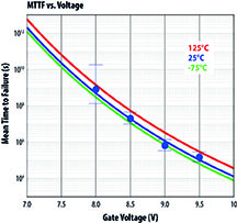
Equation 10 is plotted against the measured data points as shown in Figure 2(a), where a 1-ppm failure rate is projected for 25 years of continuous dc bias at VGS, max = 6V. The MTTF (mean time to fail) under different temperatures is shown in Figure 2(b).
During one switching period (TS), the gate mission profile can be simplified to three phases, which include overvoltage ringing due to parasitic inductance (T1), bus voltage (T2,), and off-state (VGS=0 V), as illustrated in Figure 3. By following Equation 9, Equation 11 is developed to account for the respective lifetime and duty cycle of all three phases.
![]()
where a is the duty cycle for gate overshoot, which is the ratio between T1 and TS.
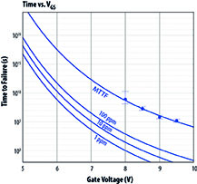
Figure 2 (a) MTTF with error bars are shown for four different voltages. The solid line corresponds to the impact ionisation lifetime model for MTTF (63.2%), 100ppm, 10ppm, and 1ppm. (b) The solid red and green lines represent the predicted lifetime at 125°C and -75°C, respectively
 Two examples, based on the data in Figure 2, demonstrate the proposed model in Equation 11. Both use 5.5V of gate bus voltage (VBus).
In the first case the gate rings to 120% of VBus, which is calculated to be 6.6V (VGS,Max = 6V). The overshoot duty cycle (a) is 1% and the device is off 50% of the time (c = 50%). According to Equation 7, b is 49%. Therefore, the device is projected to have 1.64×10⁹ seconds, equivalent of 51 years, when considering 10ppM failure rate (10 device failures per 1m devices). In the second example, a poorly designed circuit was implemented, where the gate sees a 7V overvoltage spike with 1% duty cycle (a) and 5.5V VBus with 49% duty cycle (b). After approximately 16 years, the failure rate is expected to
be 100ppM.
Conclusion
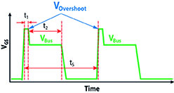
Figure 3: Normal gate switching waveform in applications, where T1 is the duration of gate overshoot, T2 is the bus voltage duration, and TS is the switching period
The test-to-fail approach applied to GaN devices to investigate the gate reliability beyond the maximum datasheet limit provides a comprehensive lifetime equation to account for the respective lifetimes under various gate bias conditions, including overvoltage stress condition and nominal bus voltage bias condition. The projected lifetime based on 1% of gate overshoot duty cycle at 120% of VBus is expected to significantly exceed 25 years with an extremely low failure rate, demonstrating the gate overvoltage robustness of GaN.