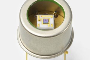
Hamamatsu Photonics has launched a TO-8 canned SPAD (single photon avalanche photodiode) with an in-built thermoelectric cooler. Called S16835, there are two models, which differ in the width* of their sensors: 54µm or 100µm. In standard operating conditions (25°C ambient, -20°C SPAD) typical dark currents are 15 or 60 count/s respectively (50 or 200 count/s max). Terminal capacitance and gain ...
Tag Archives: photonic
Single photon counting camera gets more sensitive
Edinburgh-based Photon Force has added an optics option to its single photon avalanche diode (SPAD) array camera to increase sensitivity. “Customers now have the option to specify microlensing for their SPAD array camera,” according to the company. “The microlenses offer an improvement of more than 10x in effective fill-factor, enhancing the sensitivity of the camera for time-resolved measurements. This works ...
High-volume SiN photonics foundry capacity in Europe
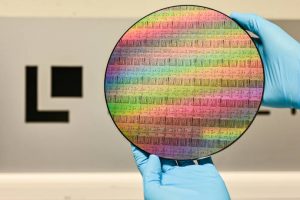
X-Fab and Ligentec have teamed up to offer “Europe’s largest capacity foundry service for integrated photonic circuits”, said X-Fab. In particular, they are talking about silicon nitride photonics, which Ligentech specialises in. “Silicon nitride offers superior performance to manage the light in the chip circuitry, with unprecedented low propagation losses and high-power handling,” said Ligentec co-founder Michael Zervas. “While there ...
UK made: Glass chip couples to optical fibres to silicon photonics
Optoscribe is sampling optical fibre to silicon photonics couplers. Branded OptoCplrLT, the devices are monolithic curved glass mirrors which turn light to direct it to or from silicon-photonic grating couplers (see diagrams). “This prevents the need for bend-tolerant fibre solutions which have some significant limitations in size and profile,” according to the company. Made using a proprietary laser writing technique, ...
SiGe, Ge-on-Si and CMOS combined at Bristol for quantum record
Researchers from the University of Bristol have made a detector to measure quantum features of light in more detail than ever before, with a sensor “clocked at an order of magnitude faster than the previous state-of-the-art,” said Bristol. It was used to measure the unique properties of ‘squeezed’ quantum light at record high speeds, according to the university’s Quantum Engineering Technology ...
Bristol university makes photons for quantum computing, on CMOS
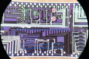
A team of physicists at the University of Bristol has used CMOS to integrate photon source suitable for “large-scale quantum photonics”, it said. “An important challenge that has limited the scaling of integrated quantum photonics has been the lack of on-chip sources able to generate high-quality single photons,” according to Bristol quantum engineer Stefano Paesani. Without low-noise photon sources, errors ...
Plasmonic receiver for last-metres mm-wave comms
Researchers at ETH Zurich have developed a plasmonic receiver that can convert millimetre waves directly into light for an optical fibre. “Our modulator is completely independent of external power supplies and, on top of that, extremely small so that it can, in principle, be mounted on any lamppost. From there, it can then receive data via microwave signals from individual ...
Perovskite solar better with silicon nano-particles
An international research group boosted perovskite solar cells efficiency by adding silicon nanoparticles. Various metal nanoparticles have been tried before, but can have drawbacks such as absorbing energy, or increasing corrosion. In the case of the silicon particles, they don’t absorb light, nor do they interact with other materials in the cell, according to ITMO University in St Petersburg, which worked ...
Wavelength-scale features lead to fast practical graphene light sensing
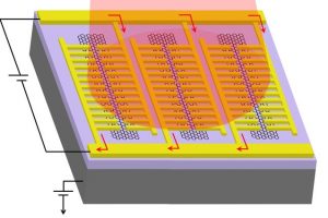
Engineers at UCLA have designed a graphene-based photodetector that is sensitive and can work anywhere in the electromagnetic spectrum from ultra-violet to microwaves. The work is published in Nature Light Science & Applications in the paper ‘Gold-patched graphene nano-stripes for high-responsivity and ultrafast photodetection from the visible to infrared regime‘, whose title explains just about all you need to know. ...
Printer for plasmonic structures works at room temperature
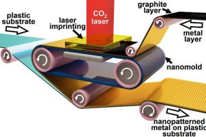
Printing nano-scale features in surfaces it difficult, according to Purdue University, particularly if the required features are smaller than the gains in the metal – the grains govern the ‘formability limit’. Sputtering metal into moulds is another route, so long at the resulting rough surface texture is not an issue. Now Purdue is claiming both a smooth surface and sub-grain-sized ...
 Electronics Weekly Electronics Design & Components Tech News
