 Test and measurement applications such as battery test, electrochemical impedance spectroscopy and semiconductor test require accurate current and voltage output DC power supplies. Both the current and voltage control accuracy of the equipment need to be better than ±0.02% of the full-scale range over a ±5°C ambient temperature change. The accuracy depends largely on the temperature drift of the current sense resistor and amplifiers.
Figure 1 shows a power supply, including an output driver, current and voltage-sensing circuits, control loops, an analogue-to-digital converter (ADC) and a digital-to-analogue converter (DAC). The selection of an output driver depends on output accuracy, noise and power level. A linear power is used as an output driver for low-power (<5W) or low noise applications. A power operational amplifier (op amp) with integrated thermal and over-current protection is suitable for low power applications.
 Using a linear output driver for higher output power is challenging because of power dissipation. A synchronous buck converter for higher output power can achieve 0.01% of full-scale range accuracy by keeping big filters at the output. For example, a 5V output range can achieve 500-µV accuracy using a buck converter. It is also important to confirm that there are no pulse-skip and diode emulation modes in the converter, which increase output ripple at light loads. Choosing a real-time microcontroller that allows the developer to disable unwanted software features is recommended for precision synchronous buck converter power supplies.
Current and voltage sensing
A high precision current shunt resistor and a low-drift instrumentation amplifier can measure the output current. The instrumentation amplifier’s input offset error and gain error are not a concern, as both errors are accounted for during system calibration. The instrumentation amplifier’s offset and gain drift, output noise and gain nonlinearity are difficult to calibrate, however, and these errors should be considered when selecting a current sense amplifier.
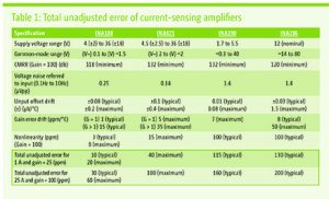
The equation below calculates the total unadjusted error of the current-sense amplifiers shown in Table 1. The error from the common-noise rejection ratio is relatively small and can be ignored.
![]() Table 1 shows the error calculations of a range of TI amplifiers. Calculations use a ±5°C temperature variation, with 100-mΩ and 1-mΩ current resistors chosen for 1-A and 25-A outputs, respectively.
Table 1 shows the error calculations of a range of TI amplifiers. Calculations use a ±5°C temperature variation, with 100-mΩ and 1-mΩ current resistors chosen for 1-A and 25-A outputs, respectively.
 Using a differential or instrumentation amplifier enables accurate monitoring of the load voltage. The amplifier senses both loads’ output voltage and ground in order to eliminate error from any voltage drop in the cables. System calibration adjusts the offset and gain errors of the amplifier, leaving only input offset drift.
The drift can be calculated in parts per million by dividing the offset drift by the full-scale voltage.
For example, with a 2.5V full-scale range and 1-µV/°C offset drift, the drift will be 0.4 ppm/°C. If you need a lower-output voltage drift, a zero-drift op amp can be selected. For most applications, however, 1-µV/°C offset drift precision op amps are sufficient.
The ADC
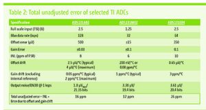
ADC offset and gain errors are adjusted during system calibration. Errors caused by drift and nonlinearity of the ADC are difficult to calibrate. Table 2 compares errors of three of TI’s precision delta sigma ADCs for a temperature variation of ±5°C. The error calculation excludes the output noise of the ADC and the voltage reference error.
Error from noise can be reduced significantly by increasing the over-sampling ratio of the ADC. A low-noise (<0.23 ppm p-p) and low-drift voltage reference (<2ppm/°C) is sufficient for DC power supply applications. For example, TI’s REF70 voltage reference has only 28ppm of long-term drift for 0 to 1,000 hours of operation. The subsequent drift therefore will be significantly lower than 28ppm for the next 1,000 hours.
Control loops
Figure 2 shows an analogue control loop for the power supply. Even if a constant-current output is not needed, keeping the constant-current loop will help with short-circuit protection. The constant-current loop will limit the output current by reducing the output voltage, and the current limit is programmable through the IREF setting.
 Using a diode inbetween the constant-current and constant-voltage loops helps with constant voltage-to-constant current transition, or vice versa. A multiplexer-friendly op amp is suitable for constant-current and constant-voltage loops to avoid a short between amplifier inputs in open loop operation. When any control loop is in an open loop condition, the op amp may see a differential voltage at its input pins greater than 0.7V. A non-multiplexer-friendly op amp has anti-parallel diodes at the input pins, which does not allow the differential voltage to exceed the diode drop. Therefore, a non-multiplexer-friendly op amp increases the bias current of the amplifier, which may cause self-heating of the device and system inaccuracies as that current interacts with source impedances.
It is also possible to implement control loops in digital domain inside real-time microcontrollers. High resolution, pulse width modulation, a precision ADC and other analogue peripherals of TI’s C2000 real-time microcontroller for example, help to reduce the total number of components and bill of materials.
In conclusion, it is important to consider temperature drift and noise specifications while designing a DC power supply for test and measurement applications. Less than 0.01% accuracy can be achieved when using a low-drift amplifier and ADC products.
 Electronics Weekly Electronics Design & Components Tech News


