 Making the correct choices will ensure your controller is market-ready by being efficient and complying with all the necessary EMC guidelines.
For DC-DC converters with relatively high inputs and outputs, filters must often be deployed at the input and output to reduce interference emissions. But it can be difficult to find a compromise between the efficiency, size, attenuation and cost of the filters, and the actual power stage – for instance using a 100W buck‑boost DC‑DC design shows what considerations should be made in terms of layout and component selection.
A hypothetical case
A typical project would be to develop a buck‑boost converter with 100W Pout at 18Vout/Vin 14‑24Vdc with 7A Iin (max) and Iout 5.55A (max) and efficiency >95% at 100W output power.
 It is also required to comply with Class B emissions (conducted and radiated) in accordance with CISPR32 have low residual ripple of the output voltage (less than 20mVpp). No shielding is possible and there will be long (1m) cables at the input and at the output. The converter must also be compact and cost-effective.
These strict requirements mean it is essential to create a very low inductive and compact layout, with filters that match the converter. In EMC terms, the input and output cables are the dominant antennae in the frequency range up to 1GHz.
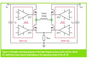
Depending on its operating mode, the converter has high-frequency current loops at the input and output (Figure 1), so both must be filtered. This prevents high frequency interference from fast mosfet switching being radiated via the cables.
This application example offers broad design freedom through a wide input voltage range up to 60Vdc with an adjustable switching frequency and the ability to drive four external mosfets.
The design is based on a double‑sided PCB with six layers and a switching frequency of 400kHz. The current ripple on at the choke should be about 30% of the rated current. The 60V mosfets feature a low through resistance (RDS(on)) and low thermal resistance (Rth).
Selecting inductors
Using the online design platform, Redexpert, the inductor can be selected. In this example, all operating parameters (input voltage Vin, switching frequency, output current Iout, output voltage Vout, and the ripple current) must be entered once for the buck and a second time for the boost operation. In buck mode, the result is a higher inductance and a smaller maximum peak current (7.52µH and 5.83A). Boost mode results in a smaller inductance, but a greater maximum peak current (4.09µH and 7.04A).
A shielded 6.8µH, 15A-rated coil from the WE-XHMI series was selected in this example. The compact device measures 15x15x10mm and has a low RDC. Its core material allows a soft and temperature-independent saturation behaviour.
Selecting capacitors
With high pulse currents through the blocking capacitors and low ripple, a combination of aluminium polymer and ceramic capacitors was selected as the best choice for this design. By determining the maximum allowed voltage ripple at the input and output, the required capacitances can be calculated as follows:
The online tool helped to determine the DC bias of the multi‑layer ceramic capacitors (MLCCs), resulting in a more practical value. A 20% lower capacitance at 24V input voltage can be expected. This results in an effective capacity of only 23µF, which is still sufficient.
Parallel to the ceramic capacitors, a 68µF/35V capacitor (in this case, the WCAP‑PSLC aluminium polymer capacitor) with a 0.22Ω SMD resistor is connected in series. This is used to maintain stability with respect to the negative input impedance of the voltage converter in combination with the input filter.
Since this capacitor is also subject to high pulse currents, an aluminium electrolytic capacitor is less suitable as it would heat up rapidly due to the higher ESR. Output capacitors are selected in the same manner.
The WCAP-PSLC 220µF/25V also provides a sufficiently fast responsiveness for transients.
The layout of the PCB also needs consideration. For example, the input and output loops that cause a high ΔI/Δt value should remain compact by locating the blocking ceramic capacitors close together. The bootstrap circuit should be compact and close to the switching regulator IC.
 A wideband Pi‑filter is necessary to decouple the internal power supply of the switching regulator. It is also advised to use as many vias as possible to establish a low‑inductance, low‑impedance connection to the internal power GND layers and the board‘s underside.
While large copper areas provide excellent heat sinks and a low RDC, they must not be too large to avoid capacitive and inductive couplings to neighbouring circuits.
EMC measurements without filter
To meet most applications, the converter should comply with the limits of Class B (household) in its interference emissions, both in the conducted (150kHz to 30MHz) and in the radiated (30MHz to 1GHz) range.
In addition to insertion loss, it is important for the high currents required that inductive components have the lowest possible RDC in order to keep the efficiency and heat within an acceptable range.
Unfortunately, a low RDC also means a larger design. Therefore, it is particularly important to use components that offer a good compromise between RDC, impedance and size.
For capacitive filter components above 10µF, inexpensive aluminium electrolytic capacitors can be used. There are no high ripple currents to contend with as the filter inductor effectively blocks these currents. Therefore, a larger ESR is not a problem, causing a lower filter quality that prevents unwanted resonances. The additional losses through the filters are due to the Ohmic losses of the inductors.
Components for input and output filters
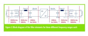
The key selection criterion for filter components is that they achieve a broadband interference suppression from 150kHz to 300MHz for conductive and radiated EMC. The filtering effort can be reduced if shorter or no cables are used at the input or output. Figure 2 shows the active ranges of the individual filter components in the respective frequency range.
 The maximum component temperature measured with a thermal imaging camera is below 64°C, which means a good safety margin for higher ambient temperatures as well as low stress for the components. The efficiency is also at a very high level (buck mode – 96.5%; boost mode – 95.6%), especially considering that all components for the filters have been taken into account.
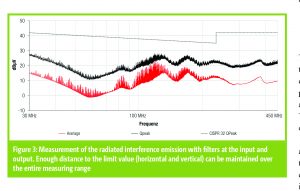
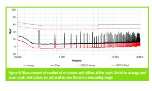
Figures 3 and 4 show the improved measurement results of the circuit with the filters in place. Figure 3 shows the measurement of the radiated interference emission with filters at the input and output. Enough distance to the limit value (horizontal and vertical) can be maintained over the measuring range.
Figure 4 shows the measurement of conducted emissions with filters at the input. Both the average and quasi-peak limit values are adhered to over the entire measuring range.
Both the clear peaks in the lower frequency range of the conductive interference radiation as well as the complete measuring curve of the radiated interference emission now exhibit enough reserve below the required limit values.
Filters for flexibility
Despite a very carefully executed layout as well as suitable active and passive components, no Class B-compliant high power DC-DC converter can be achieved without additional filters with very strict specifications, such as long lines or lack of shielding, for example.
Design and simulation software anticipated this and it was possible to lay out suitable filters in advance.
The result is a flexible, highly efficient, Class B-compliant 100W buck-boost converter. To create an even more compact PCB, the two filter banks could be turned through 90° or arranged on the underside of the PCB.
 Electronics Weekly Electronics Design & Components Tech News


