The promise of artificial intelligence (AI) and machine learning (ML) is clear. Already innovators are designing devices to anticipate our next move, analyse the world around us and respond to our voices in ways that make us safer, healthier and more productive.
We know that more can be done and will be done soon. Today, we can imagine how fully autonomous vehicles will change society. We can also envisage improved healthcare outcomes and home automation that frees humans from manual work. The challenge lies in the implementation.
Early approaches to neural networks and learning have revolved around massively parallel graphics processors (gpus) or expensive custom neural processors crunching vast amounts of data to learn and act as quickly as possible. This has worked well for forms of voice and image recognition and other applications, but a reconsideration of the status quo may also be needed.
Breaking the bottleneck
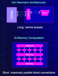
The biggest bottleneck in scaling these technologies lies in memory. Compute loads for neural networking are doubling every 3.5 months. The traditional von Neumann architecture is not very well suited for the compute requirements of neural net inference.
Moving the large volumes of coefficients (weights) and data involved between memory and the processor wastes a great deal of energy.
In current architectures, 90% of the energy for AI workloads is consumed by data movement, transferring the weights and activations between external memory, on-chip caches and finally to the computing element itself.
There are two reasons for this: first that neural net inference workloads are shaped differently from traditional ones. Traditionally a processor fetches a single, relatively small piece of data and does a large portion of the desired computation using it. With neural nets it is the opposite; every step requires parallel computation of a large amount of data with each piece of data contributing little to the final result.
Second, while transistors have shrunk in area by many orders of magnitude, the wire lengths have shrunk only linearly and the overall size of high end processors remains roughly the same. That means the energy used inside a chip has transitioned from being dominated by the transistors doing the computation to the wires that get the data to them.
To scale AI and ML and lay the foundations for new, more powerful applications, there is a need to approach the problem in a fundamentally different way, by focusing on data movement. Distance costs energy, and so every feature that an engineer adds swells the silicon area. This means data has to move farther, which slows latency, the overall cost of the chip increases because of the larger real‑estate.
Efficiency and latency
Innovators in the AI space want to improve the amount of computing they can achieve in a given power envelope. By doing more computing, they can do better inference and therefore deliver more powerful applications.
This applies to areas such as autonomous vehicles, which have constrained power budgets and, in the case of designs that are meant to go to full production, overall cost constraints that are tied in part to the electronics components inside.
In the case of power budgets, an autonomous vehicle may operate in incredibly hot environments but must function in a fail-safe mode regardless of environmental conditions. Delivering more energy-efficient subsystems is one way to tackle that challenge.
Additionally, low latency is a paramount design consideration when designing hazard-recognition systems using vision technologies. For example, a car’s camera sensor captures and analyses pixels until the AI system has determined what it is looking at. At that point it moves into decision mode. Reducing the amount of time that process takes is crucial, but can be a challenge with traditional von Neumann architectures.
Designers have attempted to break through the bottlenecks by adopting in-memory computing techniques, in which processing is improved by using analogue circuitry inside the memory array itself. In‑memory computing combines signals together and then tries to read their intensity.
That can work, but heavily relies on the specific characteristics of the process, varies as the chip temperature changes and, in the end, needs to make an approximation from the analogue signal back to a digital value. All of this makes it a difficult technology to get right, and shifting to a new process node requires considerable redesign.
A new approach
One proven approach to tackling the problem of data movement is at‑memory computation. This is a purely digital technique that is centred on minimising data movement. By tying hundreds of thousands of processing elements each directly to small, individual blocks of dedicated SRAM, the throughput of each block can be much lower while, as a system, still providing extremely high memory bandwidth.
Running standard SRAM cells next to the processing elements, at a lower speed, allows them to be run at a much lower voltage and reduces the energy costs for memory accesses. This can also cut power consumption for data transfer by up to six times.
Once coefficients and activations are loaded into SRAM, the distance the data needs to be moved is extremely short because the SRAM block and the processing element are physically abutted.
In a traditional architecture, after the expensive memory read, the data must still flow through a high‑speed memory bus with the associated energy cost of sending it that distance. The energy cost of high speed SRAM and long fast buses means that even the most advanced processes traditional architectures might perform no better than 2.5 Tops/s/W, before factoring in the cost of DRAM access.
The energy cost for retrieving coefficient data gets even higher if off‑chip DRAM is required. Most companies do not include this energy in advertised calculations, but it is a large energy cost and DRAM access is essential to making use of their architecture.
By maximising the amount of SRAM available, and keeping the coefficients on-chip, there is no external DRAM load and store. This means that the advertised energy of is the total energy it consumes. This is visible in the fact that at-memory computing designs can deliver a much higher total Top/s than other approaches, at lower power.
In cases where the neural network may be larger than a single chip, software will automatically partition the network across multiple chips in the most efficient way possible. This way even some of the largest networks can be supported.
Because the at‑memory architecture is far more efficient at getting data to where it needs to be than any other architecture, there is the option of further simplifying the processing element to save area at the expense of taking more steps to do some less frequently run operations, further increasing the efficiency of the overall system.
AI computation
The signal challenge of the AI era is how to compute vastly greater amounts than traditional computing applications have ever required. This data explosion stresses power budgets in compute systems.
At the same time, there is a requirement for vastly improved performance, since every millisecond of latency translates to less time to respond in an emergency situation, while in nominal usage it translates to a smoother overall experience.
By moving the compute element adjacent to memory cells, at‑memory architecture provides unrivalled compute density, accelerating AI inference for diverse neural networks such as vision, natural language processing and recommendation engines.
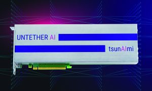
The efficiency of at-memory computation enables more processing power to be delivered in a PCI Express (PCIe) form factor and power envelope than is otherwise possible. This kind of breakthrough will herald accelerated innovation in AI that was not conceivable just a few years ago.
 Electronics Weekly Electronics Design & Components Tech News
