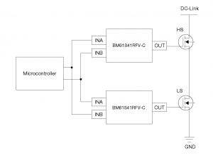
Figure 1: Cross conduction prevention circuit, using the BM61S41FV-C single channel isolated drivers
A key element in enabling these features is the isolated gate driver. Among the choices for methods to isolate a gate driver, innovations in coreless transformer technology are paving the way for compact and efficient gate drivers for high voltage systems.
The conventional isolated gate driver technology – including discrete transformer, opto‑isolated and capacitive methods, though viable in some applications – presents challenges for the latest electric vehicle (EV) and industrial power systems. For instance, discrete transformers are cost efficient, but only allow for one‑way communication from the microcontroller to the power device and not for sending information back to the microcontroller, such as temperature and over current or short circuit.
In the case of opto‑isolators, this method suffers from LED output drop from higher temperature operation and aging, which requires higher current input over time and temperature to compensate for the LED output degradation. Finally, capacitive gate drivers require a sine wave signal input to turn the output on, which may cause electromagnetic interference with wireless communications, such as Wi‑Fi.
Coreless technology

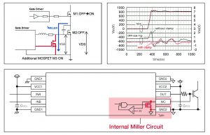
Figure 2 (top right): Measurement results when a Miller clamping circuit is used; voltage bumps are suppressed to prevent the power device from self turn on
Figure 3 (bottom): BM61S41RFV-C with integrated Milller clamp circuit
Gate drivers with coreless transformer isolation do not present any of the challenges that other isolated gate driver technologies face – they can even provide several system‑enhancing features.
There is a variety of coreless transformer implementations, but this article will look at Rohm’s which is based on three internal slabs and a low voltage section that provides a silicon interface with a DSP or microcontroller and a high voltage section that drives the IGBT or mosfet. The copper coils of the coreless transformers are separated by a slab of silicon dioxide, which is a robust dielectric with a high melting temperature and similar properties to quartz. The low voltage section operates with 3.3-5V signals, compatible with a wide range of either 3.3-5V microcontrollers or DSPs.
Unlike opto-isolator gate drivers, coreless transformer gate drivers exhibit relatively flat turn on and turn off times over temperature. Opto-isolator gate drivers tend, on the other hand, to change behaviour substantially with temperature variations that have a much longer difference between turn on and turn off times, which equates to reduced efficiency due to larger dead times.
Single channel isolated gate drivers
To drive a half-bridge, two channels are required, one low‑side and one high‑side channel. The developer is always at a conundrum to choose between a dual channel gate driver for a compact solution and two single channel drivers for the ease of layout.
In general, Rohm recommends single channel drivers (Figure 1). There are several reasons for this. The distance between two single channel drivers can be increased depending on the layout, which reduces the chances of cross talk among the channels. This can significantly reduce the need for external filter elements to realise a robust EMI design. Furthermore, the use of two independent channels offers a higher design flexibility, which is also helpful to realise a robust layout.
Cross wiring the XOR inputs of a half bridge gate driver prevents both the low‑side and high‑side from turning on simultaneously, which is a key advantage of coreless transformer gate drivers as this is not viable with opto‑isolators. Without this feature it is possible to enter a destructive mode where both the high side and low side are on simultaneously, which may even lead to a small explosion in addition to device failure.
Preventing self turn on
For typical half bridge power devices, a very sudden dV/dt in tens of nanoseconds from 0‑800V is experienced when the low side power device is shut off and the high side device is engaged with the drain voltage of the low side spiking towards the power rail.
This is problematic as the intrinsic gate‑to‑drain capacitance (Miller capacitance) of the low side device may become charged and develop a voltage bump that exceeds 2‑2.5V, approaching the turn on gate threshold voltage for the lower device.
Figure 2 depicts the developed voltage bump on the gate of the power device that was turned off. This situation could lead to shoot‑through issues where both low side and high side of the half-bridge power device is on simultaneously.
The faster the switching speed of the power device, the higher will be the amplitude of Miller current and the higher the chance of a self turn on of the power device.
Using a negative gate turn off voltage is one method of preventing this occurrence, as is using a Miller clamp.
There are additional costs and design complexities associated with the use of a negative supply, making the preferred method for many applications, where viable, the use of a Miller clamp. This is a transistor designed to provide a low resistance path from the gate of the mosfet which clamps transient voltages, preventing too high a voltage being developed from the gate to the drain of the low side device.
Figure 2 also shows the measurement results with and without a Miller clamping circuit on a BM61S41RFV‑C gate driver. The voltage bumps are suppressed, thereby preventing the power device from self turn on. In some gate drivers a Miller clamp circuit is integrated, or there is a control port available in the gate driver to drive an external mosfet of the Miller clamping circuit.
SiC power devices
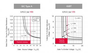
SiC power devices require higher under voltage lockout levels. Under voltage lockout (UVLO) is one of the most basic safety functions of a gate driver. It monitors the applied supply voltage and ensures that a fault is triggered as soon as the voltage drops below a certain value. This ensures that the driven power semiconductor is not destroyed by thermal overheating.
Most IGBTs are operated with a drive voltage of 15V, therefore many gate drivers with UVLO limits around 10‑12V have appeared in recent years. For most silicon based mosfets a UVLO limit of 8‑10V is sufficient.
Most SiC mosfets should be driven with higher gate voltages to ensure highest efficiency, therefore a UVLO with 10‑13V would not provide sufficient protection.
Some gate drivers have been developed with higher UVLO limits especially for this. For example, the BM61S41RFV‑C and BM61S40RFV‑C with a UVLO limit of 14.5V are pin‑compatible with the BM61M41RFV‑C with 8.5V UVLO.
This compatibility gives the designer of a power stage the flexibility to design on Si and SiC‑based mosfets.
Over voltage protection
Most gate drivers protect the driven semiconductors by means of under voltage detection but neglect the fact that the supply voltage can also be too high. This increased supply voltage is equally dangerous, as it can lead to uncontrollable short circuits or reduced lifetime of the semiconductor.
There are gate drivers which detect higher voltages. An example is the BM61S40RFV‑C which has an over‑voltage monitoring of 21.5V, allowing for a safer design.
Coreless transformer gate drivers offer features and performance advantages for EV and industrial power system applications.
High isolation voltages and pin‑to‑pin compatibility ensure safety, efficiency at system level, while providing design flexibility for off-board chargers, industrial PSUs or automotive applications like on‑board‑chargers, DC-DC converters, e‑compressor or heaters.
 Electronics Weekly Electronics Design & Components Tech News


