Nano Dimension Technologies is to develop 3D printing of advanced ceramic materials in inkjet technology for use in the aerospace industry.
Materials R&D
German researchers show double helix in semiconductors
This furry caterpillar-like image could represent an important breakthrough in flexible semiconductors for displays and solar cells. It is a semiconductor with a double helix atomic structure, similar to that which is the basis of DNA. A team from the Technical University of Munich (TUM) has discovered a double helix structure in an inorganic material. The material comprising tin, iodine ...
3D printed heatsink is worse, then better
A simple thermal annealing process could make 3D printed heatsinks better than conventional heatsinks, claims the US Oak Ridge National Laboratory. 3D printing, a type of additive manufacturing, makes it possible to produce one-piece exchangers with complex internal structures optimised to efficiently dissipate heat, but the printed material does not conduct heat as well as extruded aluminium, for example. Researcher ...
Intel invests $1.5m in IoT chip R&D in Ireland
Intel has committed to invest $1.5m over the next three years in research in semiconductor materials, devices and photonics technologies at Tyndall National Institute, the Irish ICT research institute. Intel has been investing in research at the Cork-based institute since 2009. Bernie Capraro, Research Manager, Silicon Technology at Intel Ireland, said: “The standard of work from Tyndall researchers is top-class, from ...
Comment: Brexit must not reduce research funding
Let us hope that the EU referendum in June does not have implications for the funding of research in the UK’s universities and smaller technology companies. Each year UK institutions get a share of hundreds of millions euros from the many EU research programmes. This EU cash is an important, if not vital, source of R&D funding for many universities ...
National Graphene Institute ‘almost empty’ say reports; researchers concerned about IP leaking to China
The National Graphene Institute (NGI) is deserted because the 250 Manchester University researchers working on graphene don’t trust it to keep secrets out of the hands of a Taiwanese-controlled company called BGT which has links to a mainland China university and a Chinese manufacturer, reports the Sunday Times. Is this true? “No”, replied the NGI. “How many people are working at ...
Graphene used for brain electrode in Parkinson treatment
Researchers in the UK and Italy believe a breakthrough in treatment of motor disorders, such as epilepsy or Parkinson’s disease, may be possible and with electronic neuron interface devices fabricated from pure graphene, writes Richard Wilson. Treatment of patients with motor disorders such as Parkinson’s disease could one day benefit from graphene, the highly conductive material which is expected to ...
TFETs may challenge MOSFETs
Researchers at Michigan Technological University (MTU) have developed a method for producing TFETs that overcome a key obstacle to their adoption: the need to be operated at cryogenic temperatures. Eliminating semiconductor materials in the design of their nanotube-based TFET has allowed the MTU researchers to fabricate a device that can operate at room temperatures and offers the added feature of ...
MIT fabs IC with different materials in same layer
MIT researchers have fabbed an IC by depositing ‘significantly different’ materials in the same layer, a few atoms thick. “The methodology is universal for many kinds of structures,” says researcher Xi Ling. “This offers us tremendous potential with numerous candidate materials for ultra-thin circuit design.” The technique also has implications for the development of ultra-low power, high-speed tunnelling transistors and ...
UK researchers say supercapacitor clothes can power smartphones
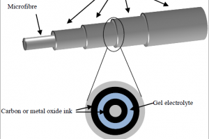
What if the materials used for clothing could be supercapacitor elements capable of powering your smartphone? This is what industrial design researchers at Brunel University London believe could be possible. Technology to produce supercapacitor thread capable of being made into cloth has been developed in the lab before but has been unable to generate the voltages needed to power smartphones. Now ...
 Electronics Weekly Electronics Design & Components Tech News
