FPGA designs for avionics applications are increasingly employing high-speed interface buses to deliver greater performance and, if the application is safety-critical, verifying the design for certification purposes is challenging.
Avionics buses use serial rather than parallel data transfer to reduce the number of wires needed in harnesses/looms, and they tend to be differential signals to reduce EMI and susceptibility. One protocol that is becoming popular in the avionics community, because of its standardisation and widespread adoption as a means of connecting devices and subsystems, is PCI Express (PCIe). It is a high-speed interface with 8b/10b or 128b/130b line encoding schemes and delivers great performance thanks to strict impedance matching. Another benefit is that clocking is embedded within the signal.
There is also a wealth of hard IP from FPGA vendors and third parties to embed. That really helps reduce the design cycle.
Analysis of a PCIe transmission at the signal level is impossible however without using additional equipment, such as a protocol analyser. It should be noted that PCIe is ‘point-to-point’, so it cannot be shared with other devices. The strict impedance matching requirements mean it is hard to physically probe for monitoring or debug purposes.
If the FPGA design is Design Assurance Level (DAL) A or B, DO-254 compliance will require in-hardware (and at-speed) testing of the target device using a requirements-based approach.
Board level test
This is the most common approach in DO-254 and is fine for simple FPGA designs. For more complicated designs, it is seldom possible to verify all FPGA level requirements due to limited access to the FPGA’s I/Os and controllability of its interfaces while on the board. One solution is to apply test vectors captured during simulation to the pins of the FPGA containing the design under test (DUT).
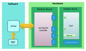
One solution, proposed by Aldec, is a compliance tool suite (CTS). This consists of a software controller, a motherboard and a daughter card (which is customised to the target design and FPGA). Test vectors captured during simulation are applied to the DUT’s pins. Simulation and physical test results are then compared. Hundreds of DAL A and B projects have been verified and this approach to verification is recognised by the certification authorities as acceptable for design assurance.
It is difficult to verify PCIe-related requirements because there is no easy way to see what the PCIe interface is doing during the test. It is possible to implement extra test mechanisms, either in software (if there is a microprocessor in the system) or in hardware, but this approach has three major drawbacks.
First, you would need to write system level test cases to test FPGA level requirements, but not all scenarios will be possible.
Second, you would need to wait for the rest of the system, with its test mechanisms, to become available. This is difficult for organisations responsible for designing just the FPGA and not the whole system. Simulation and bus functional models (BFMs) are common approaches, but they are simplified and the BFMs provided by FPGA vendors are for simulation only, not in-hardware testing. Also, for PCIe, BFMs can only validate the interfaces to the IP block. The physical layer of the protocol is not simulated.
Another approach is to perform a full simulation of the resistor-transistor logic (RTL) version of the PCIe block. Disadvantages include the length of time required and the need for extra verification IP.
Lastly, verifying designs that behave non-deterministically is a problem. There is non-determinism in the hardware, a result of data passing between different clock domains, and there is non-determinism in the execution of the software because the system is typically controlled by a non-deterministic OS kernel (such as Linux), which handles many uncorrelated events.
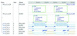
Working with test vectors and analysing design interfaces at the bit-level during in-hardware verification becomes a real challenge and obtaining repeatable consistent results might even be impossible without strictly constrained test scenarios. Typical effects of shifted or reordered data transfers observed when comparing captured bit-level waveforms are shown in Figures 1a and 1b.
Transaction level modelling
When seeking DO-254 certification authorities will typically accept simulation results as complementary evidence of verification (against requirements), but in the case of PCIe, BFM and RTL, the view is that models are still just models and in-hardware verification is required. For these reasons, operation at a higher level of abstraction is need with transaction level modelling (TLM).
A transaction is a single conceptual transfer of high-level data or a control instruction, and is defined by a begin time, an end time and attributes (which are relevant information associated with the transaction). It uses transactors, derived through a communications protocol-aware application programming interface, to interact with the DUT.
This makes possible so-called transaction-based verification. It enables the use of transactions for verification at each phase of the verification lifecycle, raises the abstraction from signal-to transaction-level, and is a natural extension of the high-level design process for very large/complex designs.
The benefits of raising abstraction to the transaction level become apparent when viewing the waveform data from Figure 1 with mismatches, but rendered to transaction abstracts, shown in Figure 2.
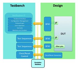
 Compared to bit-level verification, the testbench is untimed and operates using sequenced messages that bear transaction data (that is, attributes). The protocol implementation, which contains a description of the bit-level signals changing state and clocks synchronisation, is moved to transactors. In the testbench the focus is on functionality and not implementation – which aligns with DO-254, that is, specify what (the systems should do) and not how. It is also in keeping with the practices of the Universal Verification Methodology and the open source VHDL verification methodology, both of which are built around transactions.
If the DUT has asynchronous clocks and is not ready to respond to a given transaction (due to the phase differences of the clocks), it will postpone its operation. For this reason, TLM is recommended for designs with asynchronous clocks, whether high or low speed, because the modelling is more representative of real-life behaviour. Potential mismatches between simulation results (based on ideal behaviour) and in-hardware tests, which arise when transactions re-order or are delayed due to the non-deterministic behaviour, can be accommodated.
Accordingly, one thing needed for transaction-based verification is an untimed testbench, along with BFMs and verification IP.
 Under transaction-based verification the entire design is tested using transactors, and that includes the testing of low-speed interfaces and other ports (such as interrupt signals and I/O data). As in the CTS mentioned earlier it is possible to capture simulation data for in-hardware testing. This time the database contains a collection of transaction messages instead of bit-level and cycle accurate test vectors.
Following simulation of the testbench and the DUT, physical tests can be performed using the CTS (Figure 4).
 The DUT is implemented in the target FPGA located on the daughter board, while transactors (synthesisable BFMs) are implemented in a controller on the motherboard. The transactional messages from the simulation database are sent to the hardware just before the test starts, ensuring the verification is done at full speed. When the test is done, the results are gathered from hardware and saved to another simulation database for analysis.
TLM overcomes the limitations of the bit-level verification for verifying FPGA designs with high-speed interfaces and multiple asynchronous clock domains. As a methodology, which supports all HDLs, it is suitable for use with custom off-the-shelf IP blocks for interfaces such as PCIe, AXI, Ethernet and ARINC because (in cost cases) those blocks are typically delivered with BFMs and verification IP. Untimed testbenches can be used, which are easier to write, review and maintain.
 Electronics Weekly Electronics Design & Components Tech News


