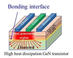
“The researchers succeed in the direct bonding of diamond and GaN at room temperature, and demonstrate that the bond can withstand heat treatments of 1,000℃, making it ideal for the high temperature fabrication process of GaN-based devices,” according to Osaka City University, home of the project.
Unsuprisingly, attempts have already been made create a GaN-on-diamond, using some form of transition or adhesion layer, but the additional layer interfered with thermal conductivity, and “due to large differences in their crystal structures and lattice constants, direct diamond growth on GaN and vice versa is impossible”, said OCU engineer Jianbo Liang.
High-temperature (typically 500℃) direct wafer bonding was a possibility, but thermal mismatch cracked the bonded result.
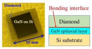 The answer was ‘surface activated bonding’ (SAB): atomically cleaning and activating the surfaces so that they react when brought into contact with each other.
“As the chemical properties of GaN are completely different from materials the research team has used in the past, after they used SAB to create the GaN-on-diamond material, they used a variety of techniques to test the stability the bonding site,” said OCU.
They used Raman spectroscopy, transmission electron microscopy and energy-dispersive x-ray spectroscopy to assess the structure and the atomic behavior of the GaN-diamond; electron energy-loss spectroscopy to reveal how the carbon atoms were bonding, and then tested the stability of the joint at 700℃ in nitrogen, as that is required when making GaN power devices.
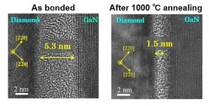 Results showed that a ~5nm thick layer of mixed amorphous carbon and diamond formed, peppered through with diffused gallium and nitrogen atoms. There was some residual compressive stress, but less than that left after crystal growth of GaN on diamond.
As annealing temperatures were increased, the layer gor thinner as amorphous carbon turned to diamond.
After annealing at 1,000℃, the layer decreased to 1.5nm, “suggesting the intermediate layer can be completely removed by optimising the annealing process,” said fellow engineer Professor Naoteru Shigekawa.
“As no peeling was observed at the heterointerface after annealing at 1000℃,” said Liang, “these results indicate that the GaN-diamond interface can withstand harsh fabrications processes.”
The work is reported in Advanced Materials as ‘Fabrication of GaN/diamond heterointerface and interfacial chemical bonding state for highly efficient device design‘.
Osaka City University worked with Tohoku University, Saga University and Adamant Namiki Precision Jewel.
 Electronics Weekly Electronics Design & Components Tech News
