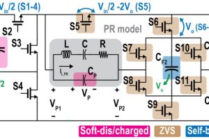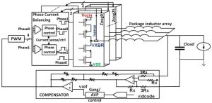
Pondering future system-in-package designs that will consume around 1kW, Intel has used a 16nm finfet cmos process to created a prototype 52 phase buck converter that can be built into such ICs, which it revealed at the International Solid-State Circuit Conference in San Francisco.
The point-of-load dc-dc takes in 2V and can deliver 200A (624A peak) at regulated sub-volt levels – operating at 200A would be compatible with a 5-year lifetime in real usage, said the company.
In the demonstration, the phases were interleaved and paralleled to form a four-phase converter switching at 65MHz. Peak efficiency is 87%.
Its passive components are MIM capacitors and one-per-phase ~2.4nH in-package inductors made from conductors and a 730μm thick magnetic layer.
Total height is ~2mm including package and ball-attach if it is configured as a stand-alone device for the back of a PCB, or it can be used as a bare-die chiplet within a stacked die system-in-module.
Circuitry on the test chip occupied 11 x 3mm of a 12 x 4mm die, and two of these were packaged with three custom test load die which provided controlled step loads for measurement.
ISSCC 2024 paper 28.6: An 87% efficient 2V-input, 200A voltage regulator chiplet enabling vertical power delivery in multi-kW systems-on-package
ISSCC, the annual International Solid-State Circuits Conference in San Francisco, is the world’s shop window for circuit advances aimed at ICs – Attendees are exposed, literally, to the state-of-the-art.
Image credit: ISSCC 2024 and Intel
 Electronics Weekly Electronics Design & Components Tech News
