In applications such as inverters, motor drives and battery chargers, silicon carbide (SiC) devices offer advantages such as higher power density, reduced cooling requirements and lower overall system cost.
Although an SiC device costs more than its silicon counterpart, the system level benefits, particularly at 1,200V, more than compensate for the higher device cost. The benefits compared to silicon are marginal at or below 600V. An SiC die needs specially designed packaging and gate drivers to reap the advantages.
Advantages of SiC over silicon
Typically, the energy lost by SiC during the reverse recovery phase is just 1% of the energy lost by silicon. The virtual absence of a tail current allows a faster turn‑off and dramatically lower losses. Since there is less energy to dissipate, an SiC device can switch at higher frequencies and improve efficiency.
The higher efficiency, smaller size and lower weight of SiC can create a higher-rated solution or a smaller design with reduced cooling requirements.
The performance of silicon worsens over higher temperatures, whereas SiC is much more stable. A silicon device is usually over-specified at room temperature to maintain specification at higher temperatures. Typically, an SiC device with half the current rating will perform the same job as a silicon IGBT because SiC is much more stable over higher temperatures and doesn’t need significant derating.
SiC operates at above 10kV, significantly above what can currently be used. SiC devices rated at 1,200V and 1,700V are available. With issues such as arcing, creepage and clearance, packaging has become the limitation – not the semiconductor technology.
Lower losses
The major sources of energy loss in an SiC module are conduction losses. As a wide bandgap material, SiC has a low gate charge, which means that SiC needs far less energy to make the device switch.
Diode switching losses are virtually eliminated because of the dramatic improvement in reverse recovery energy and tail current. Switch conduction losses are resistive and consequently are similar in both technologies. Next-generation SiC processes promise further improvement.
Higher frequencies mean reduced size and weight of the magnetics because the values of components in the transformer LC filter become significantly lower.
SiC also delivers 10x the mean time to failure (MTTF) of silicon and is 30x less sensitive to radiation and single event failure. However, SiC has a lower short circuit tolerance and hence needs a fast-acting gate driver.

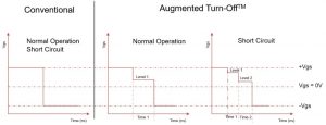
A standard, hard, turn off transition (left) and a softer stepped transition, which will reduce the di/dt
Higher frequency switching is not usually an advantage for lower-speed applications. In such situations, the cost premium of an SiC device and the additional design considerations are not justifiable, making a silicon IGBT the more logical solution.
There is also limited availability of SiC. At 600V/650V, the availability of SiC devices is low and what there is, are mostly discrete components.
A silicon IGBT requires less mitigation of RFI issues during the design process. A high-performance gate driver is not required to manage the turn-off or react rapidly to protect the device in the event of a short circuit.
Gate drivers
SiC devices need a specially designed gate driver. One designed for driving silicon IGBTs will not support the switching speed of an SiC device nor the rapid fault response time needed to protect an SiC device in the event of a short circuit.
They also require drive voltages that differ from their silicon IGBT counterparts. Voltage rails are often asymmetric and a negative rail of a few volts is usually required to hold the device fully off.
Another consideration is that SiC modules require augmented turn-off. Higher frequency/harder switching combined with lower internal losses lead to current spike and ringing problems.
Augmented or ‘soft’ turn-off uses intermediate voltage steps to manage the impact of sudden current changes and mitigate ringing. Silicon devices suffer less because of the dampening effect of internal losses.
Packaging issues
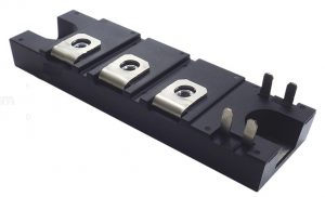
Due to the performance improvements delivered by SiC, packaging technology has now become the primary constraint – even for SiC optimised packages. SanRex (pictured), Infineon and Wolfspeed have developed proprietary SiC packages.
SiC packages are typically smaller, lower profile and more thermally efficient than silicon, although they must be designed with a symmetrical layout to minimise loop inductance. The advantages of SiC are not being realised where dies are mounted in traditional packages designed for switching at lower frequencies with more relaxed rise and fall time requirements. Non‑symmetrical designs perform badly at higher frequencies due to wave propagation effects.
If the advantages of the technology are to be realised, SiC-specific packaging and gate drivers must be used, which makes SiC a good choice for new system designs.
 Electronics Weekly Electronics Design & Components Tech News


