Fujitsu has developed a crystal structure that increases both current and voltage in GaN HEMTs, effectively tripling the output power of transistors used for transmitters in the microwave band.
GaN HEMT technology can serve as a power amplifier for equipment such as weather radar.
By applying the new technology to this area, it is expected that the observation range of the radar will be expanded by 2.3 times, enabling early detection of cumulonimbus clouds that can develop into torrential rainstorms.
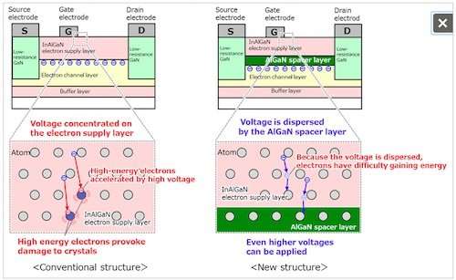
To expand the observation range of equipment like radar, it is essential to increase the output power of the transistors used in power amplifiers. With conventional technology, however, applying high voltage could easily damage the crystals that compose a transistor.
Therefore, it was technically difficult to increase current and voltage simultaneously, which is required to realise high-output power GaN HEMTs.
Fujitsu has developed a crystal structure that improves operating voltage by dispersing the applied voltage to the transistor, and thereby prevents crystal damage (patent pending).
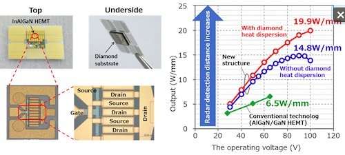
This technology has enabled Fujitsu to successfully achieve the world’s highest power density at 19.9 watts per millimeter of gate width for GaN HEMT employing indium-aluminum-gallium nitride (InAlGaN) barrier layer.
 Electronics Weekly Electronics Design & Components Tech News


