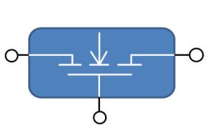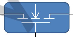
Called INN40W08, it is a 40V device that can block in both directions (unlike single silicon mosfets where two are needed for bi-directional operation).
Innoswitch announced an up-dated version here
Nominally it has a gate, two drains and no source.
The company sees it being used in high-side load switches, for over-voltage protection in phone USB ports and as a rail switch in multi-PSU systems.
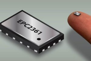
At 25°C the 2 x 2mm chip-scale device typically has 7.8mΩmax (5.5mΩ typ) on-resistance (Vg=5V), 12.7nC gate charge (Vdrain-drain=20V) and can handle 15A continuously.
As with most HEMTs, the gate needs careful control – it needs 5V gate-drain voltage to work but maximum gate-drain voltage is 6V. Peak pulsed drain-drain current can be as high as 100A and operation is over -40 to 125°C. Junction-to-board thermal resistance is 11.8°C/W.
The 40V drain-to-drain breakdown voltage is symmetrical (Idd=500μA) and zero gate voltage drain-drain current is 200μA max.
At 85°C, gate on-current is 3μA max (500nA typ) while gate reverse current (Vg=-5V) is -30μA worse case. Typical gate threshold voltage is 1.5V (Idd=1mA).
The product page is not currently available – the company is re-vamping its website.
Founded in 2015 and based in Guangdong, Innoscience (aka Innosecco (Zhuhai) Technology) makes GaN devices, including on 200mm GaN-on-silicon wafers. It has European and US offices in Leuven Belgium and Silicon Valley.
 Electronics Weekly Electronics Design & Components Tech News
