AI and software are pushing sensing and electronics to the network edge in order to provide more insights and to build models of behaviour. As a result, he believes the industry is facing three main challenges to meet “tectonic shifts” in this post-Moore’s Law era and the first decade of More Than Moore.
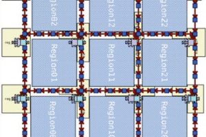
The first is x10 system scaling which exceeds Moore’s Law and which is driving the use of system in packing (SiP) as more devices are combined to create new products for systems of “unprecedented complexity”. The high levels of integration mean new packaging technologies, for example 3D packaging, are emerging. This architecture requires looking at different scenarios for a silicon strategy, the use of interposers, for example, and how to put onto a PCB, as well as reviewing packaging and board level technology.
Companies like Apple and Tesla are using their R&D spend to develop their own chips to meet processing, graphics and gaming demands. Subramanian believes that just as systems companies are taking a more holistic approach to chip development, EDA companies must do the same.
Another significant development is how AI is like electricity. It is fundamental to the new chips which lean as well as run functions. There is no getting away from AI, but the challenge is how to make it easy to use, he said.
Despite the increase in complexity every three months, there are time to market pressures, continued Subramanian. “HLS [high level synthesis] is finally coming into its prime with higher level of abstraction to describe chips.” For example, Nvidia used HLS to accelerate building blocks in its recent RC18 [inference engine] chip which was coded entirely in C++ using HLS, he reported.
“We are seeing the combination of effects of new technologies – big data, cloud and AI – driving the rapid changes in the capabilities of the devices we use and the services we can now take advantage of,” observed Subramanian. As a result, designers must think about designing a software product where the cloud is the computer, i.e., design for hundreds of thousands of node to compute and process, he said. “EDA tools have to enable x15 complexity and ensure every line is accurate to enable these products.”
He advocated a virtual model of the chip which is run on an emulator to allow the designer to see the power consumption and to analyse and debug the chip. This way, the designer can change and optimise the chip and allow a quick turnaround between the workload and the chip design.
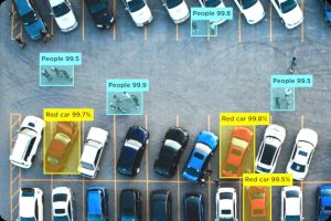
The next level is to bring a digital twin which includes sensor scenarios and sensor modelling together with a virtual model of a chip and software for object detection. This can then be processed to drive a specific instruction to control and provide a closed loop digital twin, suggested Subramanian.
“We are at the beginning of modelling based, multi-domain worlds with more hardware and software content,” he said. The multi domain environment is inevitable for systems for health, gaming, commerce or retail, automotive, the IoT or factory automation, he concluded, and this environment will need a combination of integration, tracking and analysis in chip design.
 Electronics Weekly Electronics Design & Components Tech News


