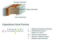
Figure 1: How capacitance is calculated (source: Murata)
Capacitors are two conducting plates, separated by an insulating dielectric layer. They hold charge when a voltage is applied to them and give up that charge when the charge-carrying electrons are given a route to flow off the plates. This charge-storing arrangement provides key circuit functions such as DC blocking, AC coupling, and energy storage and release in resonant circuits.
The practical implementation for capacitors, however, is becoming more complex as the demands of high-performance applications such as smartphones and high-performance servers are driving capacitor makers to try to increase the volumetric efficiency of the devices they offer as well as their long-term reliability. For example, manufacturers are always trying to increase the charge storage density of components so that they can offer smaller parts with the same capacitance as previous generations. Meanwhile, the challenging thermal environment of, for example, a power supply for a GPU board or server blade, is forcing capacitor makers to think hard about the long-term reliability of their components over multiple thermal cycles and the stability of performance at high temperatures.
Good capacitor design involves making well-informed trade-offs among multiple desired characteristics to achieve a balanced performance that appeals to the widest possible user base.
Capacitor basics
The quest is always to achieve greater capacity without effecting reliability. Going back to basics, the capacitance of a pair of plates separated by a dielectric material is the produce of that material’s relative permittivity, the permittivity of a vacuum, the effective area of each layer of the plates and the number of dielectric layers, divided by the thickness of the dielectric (see Figure 1). Increasing overall capacitance can be achieved by thinning the dielectric layers, increasing the number of layers, and/or increasing the effective area of the plates.
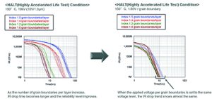
Figure 2: The number of grain boundaries per layer can affect reliability (source: Murata)
To improve the performance of multilayer ceramic capacitors (MLCCs) Murata has steadily reduced the thickness of its dielectrics from around 3µm in 1995 to less than 0.5µm today. This has steadily increased the volumetric efficiency (as expressed in µF/mm3) of the MLCCs, at the cost of increasing the strength of the electric field between the capacitors’ plates and hence the voltage stress on the dielectric material. Gains in charge density therefore must be paid for by finding dielectric materials that can withstand such increased voltage stresses while maintaining their long-term reliability.
Using conventional techniques to thin dielectric and inner electrode layers can lead to capacitors with reduced withstanding voltages, reduced reliability and increasingly voltage-dependent performance characteristics.
Murata is instead using atomisation techniques to create thinner dielectrics using ceramic materials and thinner electrodes using nickel powder. Atomising ceramic materials leads to more homogeneous and compact dielectric layers, while atomising the nickel powder allows for thinner, more even electrode layers with increased packing factors.
Materials
The way that materials are processed is at least as important as the choice of the materials themselves. Changing the size of the grains of a BaTiO3 dielectric material and hence the number of grain boundaries in each dielectric layer can alter the reliability of a capacitor (Figure 3).

Figure 3: Impact of grain sizea and dielectric layer thickness on capacitor performance (source: Murata)
Using a X7R dielectric material as a baseline, halving the thickness of the dielectric layer also halved the number of grain boundaries per unit area, undermining the reliability of the second design. Shrinking the grain size from 200nm to 100nm while maintaining the reduced thickness of the dielectric led to a net equivalent number of grain boundaries per unit area and hence similar reliability in the third design as in the base case.
This method presents a trade-off for sustaining reliability whereby there is a change in the way that the device’s performance is affected by its operating temperature. Simply put, as the grain size of the dielectric material shrinks, so does the device’s core size and its capacitance at high temperatures.
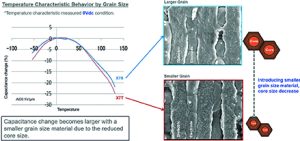
Figure 4: Relationship between grain size of dielectric material and change in capacitance at high temperatures (source: Murata)
The reliability of a capacitor (defined as its mean time to failure) is inversely proportional to the amount its capacitance changes at high temperatures. Although using smaller grains in the dielectric makes the device smaller and so more susceptible to temperature-related changes to overall device capacitance, they also allow for a smaller device that has better insulation characteristics.
Judging real-world performance
It is also important to understand the resultant characteristics in real-world use.
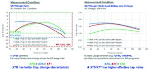
Figure 5: Capacitor performance can be assessed two ways: capacitance and temperature changes (left), and by effective capacitance in real-world use (right)
Figure 5 shows two ways of assessing a capacitor, first by how its capacitance derates at high temperatures when subject to 0V DC bias, and second by effective capacitor value under more representative, 12V DC, 10mVrms AC, operating conditions. The effective capacitance value is most useful for real design cases. It also reveals a little about the capacitor technology itself.

Figure 6: Effective capacitance measurements under real operating conditions
Figure 6 shows the areal efficiency gain made possible by shifting to smaller dielectric grain sizes (in the last column), which shows effective capacitance per unit area. Designers can use an online tool (Murata’s is SimSurfing) to explore the effect of these trade-offs on real-world designs.
One way to maintain and increase reliability is to maintain the number of grain boundaries per unit area in the dielectric layer, even if it is also being thinned. This demands the development of processes that can deposit smaller grains to form that dielectric.
The resultant increased volumetric efficiency means smaller devices of equivalent capacity to previous generations, at the cost of greater derating of capacitance at high operating temperatures. The key for designers, therefore, is to check on the device’s effective capacitance under actual usage conditions (for example, with a DC voltage applied) and across the required operating temperature. Well-designed components can provide higher effective capacitance values per unit volume than previous generations while offering the same or higher reliability.
 Electronics Weekly Electronics Design & Components Tech News
