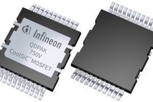
The devices “raise the benefits available from SiC technology to a new level, which has never before been possible,” says Dr. Helmut Gassel, President of Infineon’s Industrial Power Control Division.
Using SiC MOSFETs allows conversion schemes to operate at triple or more the switching frequency leading to benefits such as reducing the copper and aluminum materials used in magnetics and system housing, facilitating smaller and lighter systems for less transportation effort and easier installation.
The 1200 V SiC MOSFETs have been optimized to combine reliability with performance. They operate with ‘benchmark’ dynamic losses that are an order of magnitude lower than 1200 V silicon (Si) IGBTs. This initially supports system improvements in applications such as photovoltaic inverters, uninterruptible power supplies (UPS) or charger/storage systems, while later configurations will also extend support to industrial drives.
The MOSFETs are fully compatible with the +15 V/-5 V voltages typically used to drive IGBTs. They combine a benchmark threshold voltage rating (V th) of 4 V with short-circuit robustness required by the target applications and fully controllable dv/dt characteristics. Key benefits over Si IGBT alternatives include temperature-independent switching losses and threshold-voltage-free on-state characteristics.
The culmination of many years of experience of SiC semiconductor development, the new MOSFETs are based on a state-of-the-art trench semiconductor process and represent the latest evolution of Infineon’s comprehensive family of CoolSiCtechnologies. This family includes Schottky diodes and1200 V J-FET devices and a range of hybrid solutions that integrate a Si IGBT and SiC diode in a module device.
The first discrete 1200 V CoolSiC MOSFETs feature on-resistance (R DS(ON)) ratings of just 45 mΩ. They will be available in 3-pin and 4-pin TO-247 packages targeted at photovoltaic inverters, UPS, battery charging and energy storage applications. Both devices are ready for use in synchronous rectification schemes thanks to the integration of a commutation robust body diode operating with nearly zero reverse recovery losses.
The 4-pin package incorporates an additional (Kelvin) connection to the source, which is used as a reference potential for the gate driving voltage. By eliminating the effect of voltage drops due to source inductance, this further reduces switching losses, especially at higher switching frequencies.
Infineon has also announced 1200 V ‘Easy1B’ half-bridge and booster modules based on the SiC MOSFET technology. Combining PressFIT connections with a good thermal interface, low stray inductance and robust design, each module is available with R DS(ON) rating options of 11 mΩ and 23 mΩ.
 Electronics Weekly Electronics Design & Components Tech News


Thanks Stuart
I have changed it to SiC, from SIC
A fellow pedant 🙂
In the interests of pedantry, the headline says “SIC” – Sulfur/Iodine/Carbon – when it should be “SiC for Silicon Carbide.