This year they picked machine learning accelerators for both training and inference, an ultra-high bandwidth chip-to-chip link and an ‘infrastructure processing unit’ (IPU) for off-loading data centre management.
Tesla was invited to describe D1, the 7nm machine learning training processor used in the Dojo exa-scale computer.
D1 has 50bn transistors over 645mm2, implementing 354 compute nodes and 576 lanes of 112Gbit/s SerDes for die-die communication in a system-on-wafer package – providing 362Tflop/s total of BFP16/CFP8 processing at 2GHz.
What catches the eye about the IC is its move away from traditional global synchronous clocking.
To reduce supply current surges associated with global clocking, and therefore reduce the number of metal layers needed for power distribution, D1 uses mesochronous clock distribution.
It can do this because its nodes are in a rectangular array and node-to-node paths are only between nearest neighbours.
Essentially, a clock is introduced into the top left hand corner of the array, and each node recombines clocks from the neighbours above and to the left, and then sends its new clock down and to the right. The result is a clock wavefront spreading diagonally across the nodes from top left to bottom right.
Much of the rest of Tesla’s ISSCC paper described how this scheme was simulated and implemented in detail – metal-insulator-metal capacitors were built in the metal stack to further mitigate switching noise, for example.
 Syntiant was invited to speak about its NDP200 neural decision processor (right), which can run the MobileNetV1 network benchmark at 5frame/s for 830μW average from a 900mV core supply.
Designed for local (no cloud connection) image processing, power consumption was the key design parameter, prompting an at-memory architecture (Syntiant Core 2) to minimise the energy-sapping movement of data during inferencing.
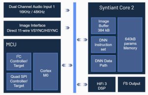
The resulting 40nm IC (left) also has a Tensilica HiFi3 DSP and an Arm Cortex M0 for additional processing.
Nvidia described its 5nm NVLink C2C chip-to-chip link that interconnects its Grace-Hopper and Grace Superchip, with 10 links delivering 900Gbyte/s between Grace and Hopper, or between two Grace chips.
It has a clock-forwarded architecture with a wide-band phase rotating phase locked loop in the receiver for per-lane skew adjustment, and wideband jitter tracking between data and clock paths.
Two of the link’s metrics are: 552Gbit/s/mm2 of chip and 40Gbit/s/pin – the latter at ≤10-15 bit error rate over a 12dB loss off-package channel. It “pushes ground-referenced single-ended link speed to 40Gbit/s with enough margin to withstand high volume manufacturing variations for off-package connections”, said Nvidia.
Lastly, Intel spoke of its IPU, and the packet processing pipeline, RDMA, storage including NVMe off-load and processing within.
“Server architectures today include disk with every server and since capacity is difficult to predict, disk storage is over-provisioned resulting in unused capacity. With an IPU, you can move to a diskless server architecture,” said Intel.
The device has 16 Arm Neoverse N1 cores, a dedicated look-aside crypto and compression
engine, three channels of either DDR4 or LPDDR4 interface, and a dedicated system management engine.
ISSCC 2023 paper 9.1: A 7nm ML training processor with wave clock distribution
ISSCC 2023 paper 9.2 A 1mW always-on computer vision deep learning neural decision processor
ISSCC 2023 paper 9.3 NVLink-C2C: A coherent off package chip-to-chip interconnect with 40Gbps/pin
single-ended signaling
ISSCC 2023 paper 9.4 An in-depth look at the Intel IPU E2000
The IEEE International Solid-State Circuits Conference, held annually in San Francisco, is a (and arguably ‘the’) world showcase for IC-based analogue, digital and RF circuity. It offers an opportunity for IC and circuit design engineers to maintain technical currency, and to network with experts.
 Electronics Weekly Electronics Design & Components Tech News
