 The adage “hardware is hard” is bound to resonate with anyone who has ever designed a PCB. Compared to software, hardware design takes more time, requires more collaborators and is significantly more prone to errors. Why is it that hardware, an industry so integral to today’s world, is so difficult despite being around for decades?
A large part of the problem is that the industry is fragmented. There is a glaring inability to collaborate, whether that is between teammates, between designers and manufacturers, or between users of the same PCB design tools.
Solving the issue of fragmentation will create a future where hardware design is as easy as software.
Fragmentation in collaboration
Team members not being able to effectively collaborate and communicate makes hardware design difficult.
A typical scenario might be two teammates, collaborating on a new board design, who realise that because PCB design tools are hosted locally, they cannot both work on the same document at the same time. To avoid conflicts, one waits for the other to finish their part of the design before making a start on their part. This means updating design files either by mailing zip files to each other or using clunky Apache subversion tools.
Meanwhile, the second partner is not entirely sure what design changes were made or why they were made. Changelogs and spreadsheets might bring some documentation to the process, but knowledge is ultimately siloed between partners. When it is time for a design review each has less insight into their partner’s work and does not catch some design errors that should have been avoided.
The next stage is to fabricate and assemble the PCB, but some design mistakes make it into the board. Then there is the second revision, where the process starts all over again.
Smooth collaboration
Collaboration should be fluid, but the bulky process outlined here just adds unnecessary hurdles. The nature of the available design tools for hardware limits the ability to work together and share information. Teams are isolated from one another and rely on antiquated methods of sharing information, inevitably leading to information loss between partners. Handling a digital hot potato of files leads to a chaotic mess of versions and lost insights. Matters are more confusing when other teams, such as firmware or mechanical ones, get involved because they don’t have the licensing necessary to access the PCB design tools.
The net result is what should be enjoyable and straightforward becomes long and tedious. Designs often take months or even years to get to market, meaning high costs and little margin for error. For a hardware startup, this isn’t only unrealistic, but it is likely to be prohibitive. No wonder there are so many more startups in software than hardware.
Supply chain fragmentation
Fragmentation exists industry-wide because so many different stakeholders are needed to bring a product to manufacturing.
 PCB design requires the physical manufacture of a board, which means relying on many disparate entities, including component manufacturers, fabrication houses and assembly houses. In an ideal world, gathering information from all these entities is a breeze, but that’s not always the case in practice.
When selecting components designers need to navigate a sea of thousands of parts from hundreds of manufacturers. To assess if a component is right for the design, it is necessary to sift through datasheets, run simulations and compare cost and sourcing availability. Once the part is selected, it is back to the PCB design tool to create a symbol, footprint and model for the part to use in the design.
Next, there are discussions with fabrication houses that will provide details about supported board stack-ups and tolerances. After finding the right fabrication house, the supported stack-up is manually entered into the design using the PCB design tool.
Finally, there is the assembly house, which supplies designers with rules and tolerances regarding component placement. These constraints must be manually added to the tool’s design rule check to ensure that the design meets all requirements for assembly.
Error-prone process
What is consistent across these examples is that all of the information a designer needs is fragmented and located outside the design tool itself. The fun part of designing hardware is doing the actual design and time away from the design tool is time not spent on design. Hunting for industry-standard information is time consuming.
In addition, this process is extremely error-prone. By all accounts, the biggest source of error in hardware design is human error. When we make the design process so manual, mistakes are sure to follow. Hardware design is already lengthy and costly enough; we need to maximise efficiency, not errors.
The current hardware design process ultimately suffers from an inability to share, collaborate and rapidly innovate. Fast iteration and design experimentation are too costly and time-consuming to pursue. This limits a hardware company’s chances of creating an economically viable product. For a startup, it limits the chances of survival.
One-tool policy
The answer is to build a single design tool that acts as a central hub for everything.
For better collaboration within the team, the tool needs to be cloud-hosted. Multiple people able to work within the same design document can cut down on the time wasted with external version control software or spreadsheets. Having one tool can offer a living version of history so that the design can act as a living changelog. All information about the design is public to everybody on the team.
Where there is more transparency in design history and decisions, teams will be better able to share knowledge, catch mistakes early on and design better hardware in less time. Design reviews will be more effective, decreasing the number of errors that reach production. By collaborating and sharing knowledge with more ease, design times can be cut in half, and a company’s chance for success doubles.
 For the big picture, zoom out to the industry level for a single tool where all entities – manufacturers, suppliers, fabrication houses, and assembly houses – can exist in a central location. The designer would not have to hunt down all of the necessary information from each of these entities. Instead, it should be the job of each group to make all necessary information publicly available and easily accessible in one place.
A designer could open up a design tool and immediately get real-time availability from a distributor, access parts with footprints and models created directly by the manufacturers, stack up pre-sets made by the fabrication houses and selectable design rules from the assembly house. There would be no need to spend time searching the web for all this information and there would be no more information loss or human error when translating the information into the design tool. Designs would be faster, errors would be less frequent and innovating in hardware would be more attainable.
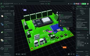
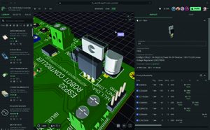
The Flux PCB design tool includes cloud hosting for live document edits between team members, real-time component pricing and availability from distributor websites and integration with leading component manufacturers. Companies such as Particle and Seeed Studio have Flux Organization pages where they directly create parts, footprints and models of their components for use by the larger Flux community.
 Electronics Weekly Electronics Design & Components Tech News


