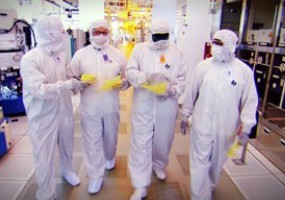
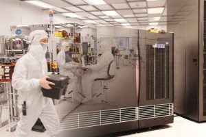
On Thursday, Hynix is to hold a ceremony to celebrate the completion of its new flash fab and the running of first silicon. The fab, designated M15 semiconductor is in Cheongju, North Chungcheong Province. It cost $13.5 billion. First silicon will be 72-layer 3D NAND. Next year it will introduce 96-layer NAND to the production mix. Samsung is building its ...
Manufacturing
Photonic ICs could decimate the cost of sensors
French research lab Leti has launched a consortium to develop mid-infra-red photonic ICs for portable optical sensors that analyse gases and liquids, initially for the petrochemical and dairy industries. The ICs, integrated on millimetre-size CMOS silicon chips, will “create extremely robust miniature systems, in which discrete components are replaced by on-chip equivalents”, said Leti. “This makes them easier to use and reduces their ...
China to have 16% of worldwide fab capacity this year
Front-end fab capacity in China will account for 16% of the world’s capacity this year, and to 20% by the end of 2020, says SEMI. China will top the rest of the world in fab investment in 2020 with more than $20 billion in spending, driven by memory and foundry projects funded by both multinational and domestic companies. SEMI’s China ...
3D printable PEEK polymer for high-performance connectors
The high-performance plastic PEEK can now be 3D printed
GloFo cans 7nm
Globalfoundries is giving up on 7nm. It will concentrate its resources on its 14/12nm Finfet process.
Challenger Solutions gets AS9100 approval
Essex-based contract electronics manufacturer (CEM) Challenger Solutions has achieved AS9100 accreditation – the extension to ISO 9000 that adds aerospace quality management standards. “Everyone gets ISO 9001,” Challenger business development manager Richard Hancock told Electronics Weekly. “AS9100 approval now allows us know to deal direct with aerospace OEM’s” The firm is mid-sized, with 85 staff. “We are big enough to ...
UK firm supplies advanced laser production facility in China
Oxford Instruments Plasma Technology (OIPT),has announced that Sino-semic have selected its Cobra plasma etch systems for their manufacturing facilities in Taizhou City. Sino-semic is a manufacturer of VCSELs for face recognition. The vertical-cavity surface-emitting laser, or VCSEL is a semiconductor laser diode which emit a perpendicular beam from the top surface, rather than the edge as in conventional semiconductor lasers. ...
Non-volatile OxRAM on multi-project wafers
French research lab Leti has teamed up with low-volume chip firm CMP to provide 200mm multi-project wafers (MPWs) including non-volatile memory OxRAM (Oxide-based Resistive Memory). “Leti’s integrated silicon memory platform is developed for backend memories and non-volatility associated with embedded designs,” said the lab. “The technology platform will be based on titanium-doped hafnium oxide [HfO2/Ti] active layers.” The OxRAM is ...
2MW battery makes and saves money at UK fab
LED-maker Plessey has added a 2MW ‘behind the meter’ (BTM) battery to its Plymouth fab. The battery power will earn revenue through a frequency response balancing contract with National Grid and help Plessey reduce its energy costs through peak-shaving of power supply in response to fluctuations in demand. Amber Infrastructure Limited provided funding for the project, which was completed by KiWi ...
Kirigami helps 3D nano-fabrication
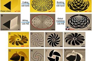
The Chinese Academy of Sciences is applying the art of Kirigami to the science of nano-scale manufacturing. The Academy’s researchers use a focused ion beam to cut a precise pattern in a free-standing gold nanofilm, then use the same beam to pull the nanopattern into a 3D shape. The pulling forces were induced by heterogeneous vacancies and the implanted ions ...
 Electronics Weekly Electronics Design & Components Tech News
