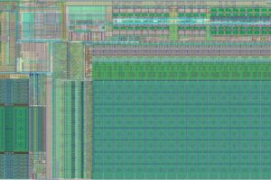
Called XT011, it “reflects the need for greater digital integration and processing capabilities within analogue applications”, said X-Fab, claiming: “It brings together the appealing attributes associated with both SoI and DTI [deep trench isolation], so that high-density digital logic and analogue functionality can be more easily incorporated in a single chip compared to traditional bulk BCD. Thermal performance has been enhanced significantly – high-current applications can be better addressed – matching what would normally be expected of a bulk BCD process.”
Standard cell library density is doubled compared with its existing 180nm XT018 BCD-on-SoI process, and it takes up 35% less area for sonos embedded flash. N-channel device on-resistance can be 25% better.
As it is a silicon-on-insulator process, parasitic bipolar effects and the risk of latch-up can be eliminated.
Devices can be made that will operate over -40 to 175°C and, for automotive use, the company can handle AEC-Q100 Grade 0 compliant designs – X-Fab is aiming predominantly at automotive ICs that include data processing, and also at industrial and medical ICs.
The PDK (process design kit) has IP (intellectual property) including sram, rom sonos-based flash and embedded eeprom.
Production will be at X-Fab’s facility in Corbeil-Essonnes near Paris, with volume production in the second half of this year.
The company has six fabs, spread across Germany, France, Malaysia and the US, with 4,200 people worldwide. It has CMOS, SoI, SiC, GaN-on-Si, mems and micro-fluidic processes, in geometries from 1µm to 110nm.
 Electronics Weekly Electronics Design & Components Tech News


