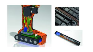
Figure 1: Applications: clamshell power tool (main), an embedded antenna in an NFC reader (top right), an electric vehicle battery pack control wiring
Design for manufacturing (DFM)’s concept’s goals are primarily productivity, repeatability, quality and, ultimately, enhancing profitability. There are examples of manufacturing concepts that create greater design freedom, sometimes making new product concepts physically or economically viable for the first time.
In the early 20th century PCBs were introduced and rapidly gained popularity as a way of replacing a lot of point-to-point wiring. Multi-layer boards represented another major step, but one that required more sophisticated schematic capture, layout and simulation tools. These, together with flexible PCB technology, which first found favour in the 1960s and 1970s, were enabling technologies without which many of the products we take for granted today could not have been created.
Surface mount components and their associated automated placement technology were enthusiastically embraced from around the mid-1980s. They also heralded new opportunities for creative electronic product design.
Over the last century manufacturing automation has advanced, with PCBs as the universal foundation of many electronic products, but the wire (or cable) harnesses needed to connect one part of a product to another have remained a significant barrier to full manufacturing automation.
A recent development in additive manufacturing (AM) technology, however, promises to eliminate, or at least mitigate, the design and manufacturing limitations created by the need for wire harness interconnect.
3D additive manufacturing
AM, the most common form of which is 3D printing, is a process of creating objects by adding layers of material based on a digital model. It allows for complex and intricate designs and enables rapid prototyping, reducing time and costs for iterative design and development. AM can improve supply chain efficiency by enabling on-demand and localised production; it also facilitates rapid customisation. It has been widely adopted in the aerospace and automotive sectors.

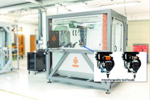
Figure 2: A five-axis additive manufacturing robotic cell
Most 3D products produced using AM are made using three-axis printers but, more recently, five-axis machines have become popular because they permit more complex shapes to be produced. Sometimes they enable multiple components to be consolidated into one piece and they can improve both the structural integrity and surface finishes of products. Five-axis machines minimise materials wastage by eliminating the support structures needed for some 3D-printed products.
Whether products are made using AM or other techniques, connecting them using wire harnesses poses several challenges. Harnesses are made by hand, making them expensive and prone to errors during manufacture. Most are made in countries with low-cost labour and so have to be transported, sometimes thousands of miles, making the supply chain complex and costly.
Wire harnesses are flexible and rarely anchored along their whole length. As a result, in many transportation and industrial applications, they are prone to chaffing and insulation damage whenever they are moved, intentionally or otherwise. This means that system designers may need to over-specify wiring to ensure reliability, considering mechanical as well as electrical factors. Conductors may have to be of a heavier gauge than strictly required for their current-carrying capabilities and insulation may need to be thicker. Both factors add cost and weight, a particular problem in automotive and aerospace manufacturing, but also an important consideration in most industrial and consumer products.
Robotic integration
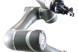
Electrical function integration may eliminate these and other design constraints. The most recent five-axis robots have moved beyond simply building composite structures (Figure 1). They can now lay down electrical conductors within the structure of composite products using dedicated robotic heads called end effectors. The conductors may be bare wires up to 3mm in diameter or insulated wires, and terminations can be printed into the structure too. The conductors will carry power at currents of 10A or more, data, or signals, and the process can be applied directly to flat or curved surfaces. This technique is known as electrical function integration.
Composite materials, insulated wires, bare wires and interconnect components can now be assembled in a fully-automated, AM process.

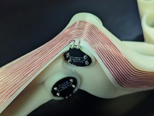
Figure 3: AM allows conductors to be automatically placed even in curved surfaces
Commercial benefits are improved product quality and consistency and increased manufacturing throughput. Electrical function integration also has profound implications for system design anywhere that a wire harness may previously have been used. The path of integrated conductors can be accurately defined with the composite structures to which they are applied, meaning that the shortest viable routes within a product can be used. Careful design can therefore minimise both series inductance and capacitive coupling between conductors, and resistive losses. Figure 3 shows a control grip with conductors automatically placed into a product, even where complex curved surfaces are present.
The conductors can be accurately set within printed channels created in the body of the product and, where needed, they may be further secured by printing tiny composite fixings over the top of the wires.
Weighing up benefits
The wires are so well fixed that bare wires may be used where insulated types are needed in conventional harnesses. The wires are not going to touch, so there is no possibility of short circuits. There is no need to over-specify the conductor diameter because functionally integrated wiring is not subject to the same mechanical stresses as a conventional wire harness. Both of these factors can save considerable weight.
In an evaluation of the technology for replacing the wiring in a business-class airline seat, weight savings of at least 5kg per seat were deemed possible. Benefits to aircraft and other forms of transportation are increased range for a given amount of fuel or each battery charge, lowering CO2 emissions.
Weight reduction also creates new design opportunities. For example, handheld power tools, aircraft simulator grips or game controllers, many of which use a clamshell design, may be more attractive to customers if they are lighter and less tiring to use. Alternatively, greater electronic functionality can be added to differentiate these devices without making them excessively heavy.
The same benefits apply to the size of a product. With no need to make mechanical design compromises to accommodate traditional excessively bulky wiring and connectors, products can be made more compact. Space savings created by this electrical function integration may present opportunities for adding more functions, perhaps enabling more user controls or interfaces to be introduced without exceeding the physical size or form factor goals for a product.
The mechanical constraints that are eliminated by electrical function integration will enable new physical form factors to be explored for many products without adding unacceptable cost, weight or size.
These opportunities will be amplified by today’s trend for electronics design engineers to become multi-disciplined. They are increasingly taking a holistic approach to product design, spanning electronic hardware, software and mechanical engineering.
The next design revolution?
PCBs and flexible circuits transformed electronic design in the first 75 years of the last century. Surface mount technologies, including components and new levels of automation in manufacturing, had a similarly revolutionary impact on design during the final quarter century of the last millennium. It will be fascinating to see what the creativity of the electronic design community will make of the new opportunities presented by electrical function integration.
 Electronics Weekly Electronics Design & Components Tech News


